Timing Diagrams
Figure 2.10
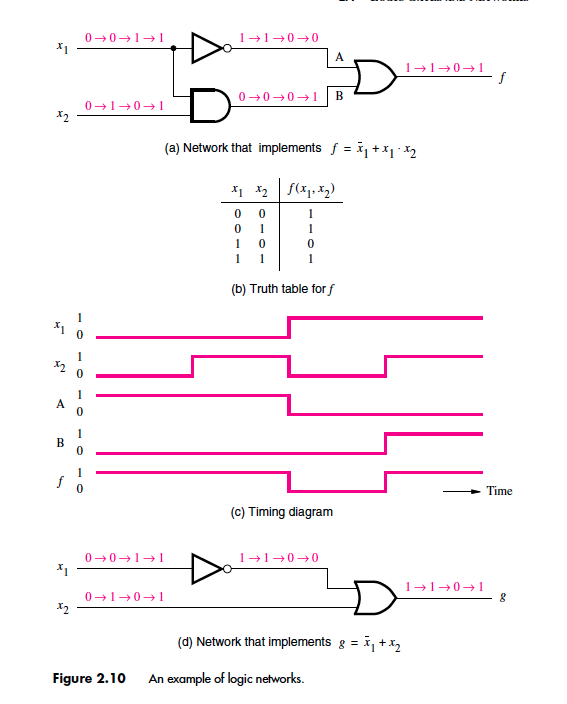
We can determine the behavior of the network in Figure 2.10a by considering the
four possible valuations of the inputs x1 and x2. Suppose that the signals that
correspond to these valuations are applied to the network in the order of our
discussion; that is, (x1, x2) = (0, 0) followed by (0, 1), (1, 0), and (1, 1).
Then changes in the signals at various points in the network would be as
indicated in blue in the figure. The same information can be presented in
graphical form, known as a timing diagram, as shown in Figure 2.10c. The time
runs from left to right, and each input valuation is held for some fixed period.
The figure shows the waveforms for the inputs and output of the network, as well
as for the internal signals at the points labeled A and B.
Timing diagrams are used for many purposes. They depict the behavior of a logic
circuit in a form that can be observed when the circuit is tested using
instruments such as logic analyzers and oscilloscopes. Also, they are often
generated by CAD tools to show the designer how a given circuit is expected to
behave before it is actually implemented electronically.